
2012
![]()

Development of “Fine Micro Patterning Equipment”May 23, 2012
[Capable of imaging patterns with a line width of 10 μm or less, helping to increase FPD productivity]
NTN Corporation (hereafter, NTN) has developed the “Fine Micro Patterning Equipment” that allows patterns with line width of 10 μm or less to be imaged.
NTN has developed devices capable of repairing color defects in flat panel displays (hereafter, FPD), which helped to increase productivity for customers. Yet with the the conventional needle method, where ink adhered to the needle tip is transferred to the the substrate following contact, the pasted diameter of the ink was slightly larger than the diameter of the needle tip. In order to repair patterns with line widths of 10 μm or less, expensive and complex devices such as the laser CVD* were required.
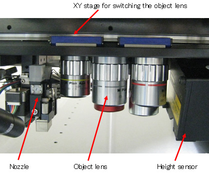
The newly developed “Fine Micro Patterning Equipment” employs an electrostatic ink jet method that is capable of imaging microscopic patterns on substrates without any contact. The electrostatic ink jet method is an application method that sprays ink from microscopic nozzles using electrostatic suction, and allows imaging of line widths of 10 μm or less that was not possible with needle method. The device features a relatively low-cost and simple structure compared to industry-standard devices used for repairing line widths of 10 μm or less, and also increases imaging speed.
The device features a range of newly developed technologies, including a one-touch release mechanism that allows the nozzles to be attached and released easily, a collision prevention function between the nozzle and substrate, imaging instruction function using a mouse with a display on a monitor, and a localized baking function used to instantly harden ink with a laser after imaging is complete. These combine to create a high-productivity device with outstanding operation and maintenance capabilities.
NTN plans to market the developed product globally as a product that can contribute to increased productivity of smartphones, tablet terminals and organic EL substrates that are growing in demand around the world.
* Laser CVD (Chemical Vapor Deposition): a film formation method where a metallic film develops on the surface of a substrate when the substrate placed within an atmosphere of the source gas is exposed with a laser, which triggers a chemical reaction with the metallic substances contained within the source gas.
Features
- The use of an electrostatic ink jet means patterns with line widths of 10 μm or less can be imaged without any contact
- High-productivity FPD repair system with outstanding operation and maintenance capabilities
- One-touch nozzle release mechanism using magnets
- Equipped with a collision prevention function between the nozzle and substrate
- Defects displayed on a monitor screen can be imaged using mouse operations
- Equipped with a localized baking function to harden ink instantly with a laser after imaging
- Can be used with large substrates when combined with large tables
Applications
- Repairs of FPD substrate wiring Eg.) Repairs of TFT substrate wiring
- Repairs of patters of photo mask substrates for exposures
- Ink dispensing, pattern imaging, etc.
Inquiries about this release
Product Photo
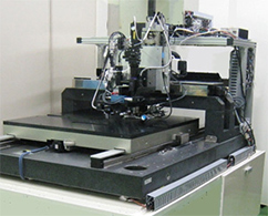
Fine Micro Patterning Equipment (main parts of device)
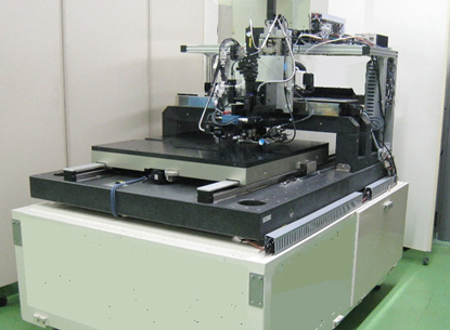
Example of installed Fine Micro Patterning Equipment
Application: repairs of FPD substrate wiring (example)
![]()